#20 Characterizing and Modeling Non-Volatile Memory Systems
14 Oct 2021
| Link | https://swanson.ucsd.edu/data/bib/pdfs/MICRO20-LensVans.pdf |
| Year | MICRO 2020 |
Summary
This paper contains two main components: LENS and VANS. LENS is a profiler used to extract key NVM microarchitecture parameters by executing microbenchmarks on real NVMs. VANS uses parameter acquired from LENS to build a NVM simluator. The authors show that this approach offers higher simulation accuracy compared to prior models such as DRAM+delays.
Background
Details
Internal Buffers
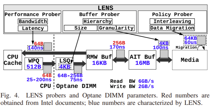
Based on released Intel documents, the paper identifies several known NVM architecture components.
- Write Pending Queue (WPQ): a queue in the memory controller that stores pending NVM write quests. This queue is in the ADR domain, meaning that it is power-fail safe.
- Load Store Queue (LSQ): queue that reorders incoming read/write requests. This queue also performs write combining. The goal is to minimize read-modify-write operations.
- Read Modify Write buffer (RMW): buffer that performs RMW operations. Recall that the underlying NVM media has 256 Bytes granularity. Also recall that Intel cache line size is 64 Bytes. If the LSQ fails to combine multiple 64B requests into a 256B req, then we need to perform RMW operations. This makes sense. If we are writing less than 256B, we need to know what the original NVM content is. RMW is of course more expensive than a write due to the extra read and modify operations.
- Address Indirection Translation buffer (AIT): buffer that performs internal address translation to achieve wear-leveling and bad-block management.
Prior NVM Simulators
Prior emulators work by stalling CPU for additional cycles or injecting software delays. This approach is NOT accurate and cannot more NVM’s complex performance behaviors. The paper gives two discrepancy examples. 1) inaccurate BW and latency magnitudes 2) real NVMs have unstable read latencies.
LENS profiler
THe main goal of LENS is to inject specially designed microbenchmarks to reverse engineer NVM architectual parameters.
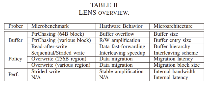
Benchmarks:
- Pointer chasing: allocates a continuous NVM memory region (PC-Region). Divide it into equal sized
blocks (PC-Blocks). Perform R/W on all blocks in the region in a random order. Sequentially access data
within each block. Three variants:
1) Buffer capacity: fix block size, vary region size and collect average latency per cache line
2) Buffer entry size: fix region size, vary block size
3) Issue read after write reqs
- All accesses bypass the cache
- Overwrite: repeated write to a fixed NVM region. Two variants: 1) collect execution time of each write in fixed region 2) measure frequency of long tail-latency by changing region size
- Stride: r/w cache lines with fixed stride. Two variants: 1) fix stride, vary access size, and measure BW 2) fix access size and vary stride to cahcaterize interleaving
Here is how the paper probes each parameters:
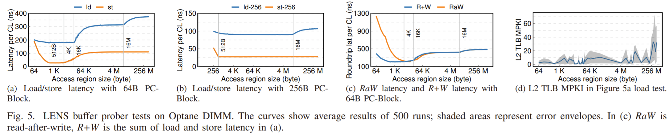
- Buffer capacity:
- For the two read buffers, RMW and AIT, we can think of them as caches. When the CPU requests 64B of data, we can return from RMW if the entry exists in the buffer. The pointer chasing benchmark RANDOMLY accesses blocks within the memory region. If the region size is larger than the RMW buffer capacity, we will need to eventually evict lines from the buffer. The CPU may make another data request in the already evicted cache line, causing higher latencies (Credit to my colleague for helping me understand this).
- For the write buffers, WPQ and LSQ, here is my guess on why Figure 5a appears the way it is. As the region size approaches the WPQ size (512B), the latency improves because there are more write coaleasing opportunities. When the region size exceeds 512B, the speed up stops because the CPU must wait for the WPQ to free up before inserting more write requests.
- Buffer entry size:
- Measure r/w amplificaiton while varying the size of PC-Block. Ex. if the buffer entry size is 256B and the block size is 64B, then we will get a read amp of 4x. If we increase the block size to 256B, the read amp is 1x, meaning that the block size equals the buffer entry size. Note that this works because accesses within each block is sequential. This means that if the block size is 256B, even though the CPU cache size is 64B, we still have a read amp of 1x because we can reuse the 256B line in the RMW buffer.
- Buffer hierarchy:
- I do not understand what the paper mean by independent buffers and why “Independent buffers can fast-forward data from each buffer in parallel.” Do they mean exclusive buffers?
- Migration freqeuncy:
- Overwrite to the same memory region repeatedly. If a migration occurs, the write latency would suddenly spike up. This is because once a migraiton occurs, subsequent writes must wait for the migration to complete before proceeding.
- “Typical NVRAM wear-leveling schemes migrate data from one NVRAM media location to another to maintain evenly distributed wear out.” Why is migration needed? I thought wear leveling just updates the logical to physical address table.
Workload Studies
The paper notes two primary sources of inefficiency:
- Read misses caused by pointer chasing access pattern, which is common for data structures such as B-Tree. Read operations dominate NVM Redis execution overhead, having an 8.8x higher CPI than other operations.
- Write amplification overhead: Most writes in YCSB are concentrated in only ten cache lines, but they trigger 503x more wear leveling!
Questions
- If the NVM media is 256-byte access granularity, how is it byte-addressable?
- See buffer hierarchy
- The paper claims that buffer overflows will cause dramatic change in access latency. Why is the latency dramatically different when a buffer overflows?
- See migration freqeuncy
Further Readings/Topics
- B-Tree in cloud workloads
Sources
[1] https://www.intel.com/content/www/us/en/developer/articles/technical/deprecate-pcommit-instruction.html